Why sometimes it is obvious that the PCB design has not checked out the error, but there are still bad situations such as short circuits and broken boards after production and processing?
That’s because you didn’t take into account the hole spacing, resulting in unavoidable loss during assembly.
In the production of single-sided or double-sided PCBs, the non-conducting holes or conducting holes are directly drilled after blanking; the multi-layer boards are drilled after the pressing board is completed.
According to the function, drilling can be divided into the part hole, tool hole, through the hole, blind hole, and buried hole. Conventional drilling is processed by drilling machinery. In actual processing, the distance between the drilling holes usually affects the processing of the drilling machine and the reliability of the finished product.
Therefore, when designing, the actual processing situation of the hole spacing must be taken into account:
VIA (commonly known as a conductive hole)
Minimum hole diameter: mechanical drill 0.15mm, laser drill 0.075mm; minimum via hole diameter not less than 0.2mm. The distance between the pad and the contour line is 0.2mm; the single side of the pad should not be less than 4mil, preferably greater than 6mil, and the hole-to-hole spacing (hole edge-to-hole ) should not be less than 6mil, preferably greater than 8mil.
PAD pad hole (commonly known as a plug-in hole)
The distance between the pad and the contour line is 0.25mm; the single side of the outer ring of the pad cannot be less than 0.15mm. The size of the plug-in hole must be more than 0.2mm larger than the pins of the DIP component, so as to prevent the difficulty of inserting into the hole due to processing tolerances
Non-metallic holes and slots (commonly known as copper-free holes and slots)
The minimum spacing of the slot holes is not less than 1.6mm, otherwise, it will cause holes to increase the difficulty of edge milling. The distance between the slot hole and the edge of the board is not less than 2.0mm, otherwise, it will cause holes.
The longer the non-metallic slot, the greater the distance from the edge of the board, so as to prevent the remaining board edge from disconnecting the stamp hole as a bridge between the board and the board. , If the spacing is small, it is easy to break the board, if the spacing is too large, it cannot be broken, so the spacing is 0.2–0.3mm.
Since there are so many issues that need attention, how can we comprehensively and conveniently consider the manufacturability of all hole spacings at one time?
DFM Manufacturability Check of Hole Pitch
- Via the same network
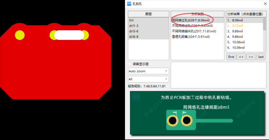
If the two holes are too close during the drilling operation, it will affect the timeliness of the PCB drilling process.
After the first hole is drilled, the material on one side will be too thin when the second hole is drilled, resulting in an uneven force on the drill tip and uneven heat dissipation of the drill tip, resulting in a broken drill tip, resulting in the collapse of the PCB hole. Beautiful or missing drill holes are not conducive.
- Different network vias
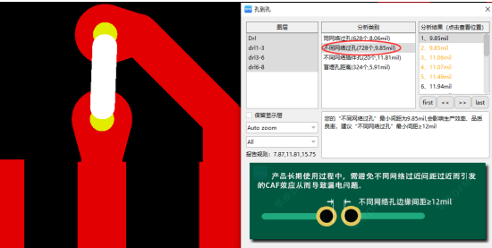
The via holes in the PCB board need to have an annular ring on each layer of the circuit, and the surrounding environment of each layer of the annular ring is different, with or without clamping lines.
In the case of ensuring the spacing, a part of the annular ring that is too close to the clip line or the hole is too close to the hole will be cut off to ensure a safe distance of 3mil from the soldering ring to the copper/wire of different networks.
If the via hole spacing of different networks is small, the safety spacing is insufficient and it is easy to short circuit.
- Different network plug-in holes
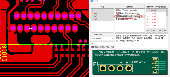
There will be a small amount of offset in the same direction in PCB production. When the spacing between plug-in holes of different networks is small, the pads of the plug-in holes will be cut to ensure safe spacing.
The direction in which the pad is cut is irregular, and the worst phenomenon will cause the hole to break the welding ring, or short circuit with tin during welding.
- Blind buried hole distance
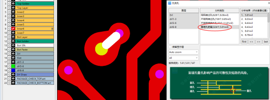
A blind hole is a type of via that connects the inner layer of the PCB to the surface of the PCB. This hole does not penetrate the entire board; the buried hole is a type of via that only connects the traces between the inner layers, so it is from the surface of the PCB.
It cannot be seen; the distance between blind holes and buried holes is too small or there is no distance, which is called stacked holes. According to the law of PCB lamination, the design of stacked holes may not be convenient for production.
When the lamination method cannot make the overlapping parts of the blind holes and buried holes in the same network drill through and connect, it is necessary to go through the stacked hole process. After the buried holes are completed Electroplating, lamination, and drilling of blind vias.