
Electrostatic discharge (ESD) is a pervasive threat in electronic circuit design, capable of damaging expensive components or causing subtle system failures that are difficult to diagnose.
Many engineers are familiar with basic ESD precautions. Typical examples include wrist straps and conductive mats.
However, designing circuits to resist ESD events and maintain normal operation demands a more systematic approach.
This article examines the fundamental characteristics of ESD behavior.
The discussion ranges from the Human Body Model and Machine Model to voltage clamping and ground bounce effects.
It further introduces practical design strategies.
These strategies cover board-level fortress architecture, TVS diode selection, communication port protection and firmware-level intelligence.
The content offers engineers a complete framework to develop electronic systems capable of resisting ESD interference.
How Can We Prevent Electrostatic Discharge (ESD) in Circuit Design?
We have all encountered electrostatic discharge (ESD) at one time or another.
A typical scenario is walking across a carpet and then touching a metal component.
This action can instantly release accumulated static electricity.
Many of us have complained about having to use conductive mats, ESD wrist straps, and other measures in the lab to meet industrial ESD standards.
Many of us have also damaged expensive electronic components due to careless handling of unprotected circuits.
For some, ESD poses a challenge because it requires handling and assembling unprotected electronic components without causing any damage.
ESD creates a major challenge for circuit design. Designers must guarantee that the system survives an ESD event.
The system should keep working properly after the interference.
Ideally, users should not notice any failures triggered by the ESD event.
Contrary to common belief, designers can indeed ensure that a system remains operational and free of failures after an ESD event.
Keeping this goal in mind, let’s first gain a better understanding of what actually happens during an ESD event, and then explore how to design the proper system architecture to address ESD.
Simple Model
Researchers charge a capacitor to a high voltage (typically 2 kV to 8 kV).
They close a switch to discharge the charge into the device under test. This device is built to withstand the ESD surge (Figure 1).
The charge may be positive or negative. Designers need to address both positive and negative ESD scenarios at the same time.
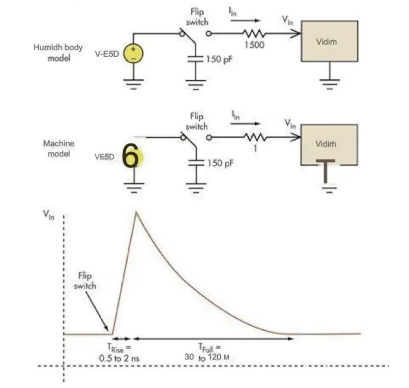
High transient voltages that damage circuits typically have a rise time of several nanoseconds and a discharge time of approximately 100 nanoseconds.
Different damaged circuits may vary significantly in their sensitivity to positive and negative surges; therefore, you need to properly address both types of surges simultaneously.
The difference between the two most common models—the Human Body Model (HBM) and the Machine Model (MM)—lies primarily in the series resistance. The HBM is not as conductive as metal.
The best protection against overvoltage damage is to use nonlinear circuits for voltage limiting or clamping (Figure 2).
Engineers widely adopt specialized diodes. These components exhibit very low impedance under forward bias or within the Zener breakdown region.
Introducing a voltage limiter can rapidly trigger certain other events, as large surge currents flow through the limiter during capacitor discharge.
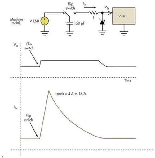
Although high transient voltages are eliminated, the resulting surge currents of several amperes may cause other problems in the system.
Depending on the total impedance of the subsequent path, surge currents can reach several amperes.
When designing I/O units for chips, it is common to see surge currents of 4 A to 16 A entering the device.
Handling such large transient surge currents has become a major challenge in ESD design.
Limiting voltage is relatively straightforward, but the resulting current can cause reverse polarity between circuits and ground elsewhere in the system.
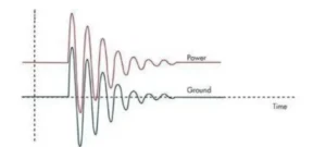
The current forced to ground by the voltage limiter will induce ringing at that node in the system (Figure 3).
The voltage typically propagates along the ground path and is a function of the power supply decoupling capacitors, so the system core continues to function normally.
However, control lines connected to the circuit board may become disrupted because they are referenced to ground outside the board.
As a result, an ESD event may occur at a certain location, causing an input on the circuit board to appear faulty.
Role of a Fortress
Using board-level ESD protection, you can attempt to build a fortress and establish multiple controlled access points along the “moat.”
Engineers can broadly classify components connected outside the “walls” into several categories.
These categories include protocol-controlled data, low-bandwidth sensing and control lines, and high-speed interfaces.
The first two are relatively easy to handle, while the third presents a certain degree of challenge.
There are several different methods to protect these three components from ESD damage.
Regardless of the final product’s design, some form of protective enclosure will be part of the device.
Isolating the circuits inside the enclosure is the first line of defense that requires careful consideration.
Ideally, the metal enclosure surrounding the circuit board is usually sufficient, but modern products often use non-conductive plastics or other modern materials.
Circuit designers generally have no control over the materials used to build the “walls,” but they bear an inescapable responsibility for protecting the “fortress.”
When designing the enclosure, it is important to note that any ESD reaching any part of the exterior of the enclosure has countless paths to enter the internal circuitry.
Building a PCB that acts as a fortress capable of defending itself against ESD surges can begin with a low-impedance grounding strategy.
Designers can build a solid ground plane and maintain good power integrity.
This enables the printed circuit board (PCB) to maintain signal integrity over the whole board.
The PCB can stay stable even under large ground surge currents.
As a design engineer, you would require everyone to fasten their seatbelts to withstand minor turbulence.
The aircraft may bounce up and down rapidly, but if everyone has their seatbelts fastened, everyone will remain secured in place, and the aircraft will continue flying.
After that, you need to protect external connections and limit the effects of ESD events.
Designers should place protective circuits at the board’s entry points instead of downstream locations.
Engineers may need to deal with several thousand volts of potential generated by arcing, or surge currents of several amperes.
They can best manage these risks right at the board’s edges.
TVS Voltage Limiters
Designers can use Transient Voltage Suppression (TVS) diodes as voltage limiters.
Engineers classify these devices according to general-purpose voltage, logic levels, and power supply voltage.
Common voltage types include: 12V, 5V, 3.3V, 2.5V, 1.8V, and 1.2V.
Designers will find these voltage values familiar. Manufacturers specifically develop these devices to satisfy the requirements of numerous CMOS components.
No single specification suits every application. Engineers must select devices rated to match the operating voltage of the circuits under protection.
Modern CMOS processes have significantly reduced supply voltages to protect transistors that have limited design margins and a narrow voltage range—a feat worthy of our respect.
These devices are typically manufactured using foundry processes that can provide high-current devices with low impedance characteristics in small packages.
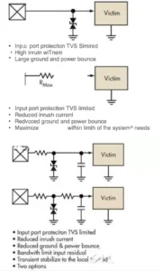
Placing a TVS voltage limiter on the input line can protect the input from destructive ESD damage (Figure 4).
However, such a limiter cannot handle signal glitches that occur during host processing, nor can it address the reverse-bias effect caused by massive ground current surges.
As mentioned earlier, there is a significant difference in performance between HBM and MM.
In many cases, adding some series resistance before the TVS device helps limit current surges and reduce ground bounce.
As with HBM, the end result is reduced system stress.
Bandwidth limiting alone typically does not solve ESD problems.
Low-pass filters also require attenuation of 60 dB to 150 dB to eliminate transient voltages from small ESD events, which is difficult to achieve with simple passive filters.
TVS protectors can pull the signal down to the power rail level.
A first-order RC circuit can then be used to maintain signal integrity (Figure 4).
Capacitors can also stabilize the input voltage relative to local ground.
This approach provides excellent protection for a large number of low-bandwidth inputs, including “set-and-forget” control lines, sensor inputs, and similar components.
Although most of our discussion has focused on protecting PCB input ports, output port protection follows a similar principle.
TVS diodes and additional resistors are also well-suited for this purpose.
Limiting the voltage helps prevent semiconductor damage and protects other components with voltage limits.
Series resistors also help stabilize the ground.
In addition, designers can divert ESD surge current away from the I/O units of digital chips.
This prevents ground bounce from occurring inside these chips. The processor can therefore keep running normally.
Meanwhile, the external voltage limiter absorbs the surge current.
ESD Within the Chip
For a variety of reasons, ESD protection within ICs involves some trade-offs.
Manufacturers optimize silicon and metal materials to fulfill an IC’s core functions. These materials cannot adapt to high-current operation.
Dedicated TVS devices use silicon optimized for high-current circuits and offer higher performance than the PN junctions found in standard CMOS.
Furthermore, I/O cells with high-current ESD protection occupy a significant amount of space, thereby increasing the cost of the IC.
Moreover, high-frequency pins on an IC typically cannot accommodate large ESD protection circuits, as these would introduce a capacitive load.
As a general rule, the level of on-chip ESD protection is sufficient only to complete IC manufacturing and solder the IC onto a PCB;
It lacks the robust protection typically required in the application environment.
If circuits run outside the PCB, designers usually adopt external devices to offer extra protection.
Data Communication Ports
Properly designed communication ports use robust protocols that incorporate the widespread use of cyclic redundancy check (CRC) coding to verify data integrity.
Ethernet, USB, and CAN bus all employ CRC coding, which is transmitted along with the data.
A properly designed receiver checks whether the CRC code matches the transmitted data.
If a mismatch occurs, it means errors exist in the data or the CRC code. The system sends out a request to retransmit the data.
Since ESD events last less than 100 ns, the CRC check, validation, and retransmission process typically handles ESD in an imperceptible manner.
End users generally do not realize the system has corrected corrupted data.
Some other protocols lack such protective measures in their design.
I²C, Serial Peripheral Interface (SPI), and System Management Bus (SMBus) communication designs operate on the PCB and cannot verify or correct data.
If data is to leave the board, ensure you have a method to verify its validity.
Most modern communication paths use a differential configuration, specifically some form of low-voltage differential signaling (LVDS).
Designers must protect every LVDS connection with a TVS device, the same way they handle all other signals.
Magnetic isolation (commonly used in Ethernet) and common-mode chokes help address common-mode variations caused by ground bounce during ESD events.
Designers should implement optical isolation or magnetic isolation.
They take this measure when the input signal shares a different ground from the PCB.
High-speed data streams that require robust data integrity but do not include error detection are particularly challenging to protect against ESD surges.
Understanding how devices provide serial data rates exceeding 1 GB/s and comprehensive communication protocol protection can help avoid this issue.
Analog Signals and Digital Intelligence
Any analog signal entering or leaving a circuit board requires basic TVS protection.
Designers must consider the bandwidth of the connection channel.
They use this information to decide whether to adopt any extra measures.
Most analog control signals, motion control systems, audio, and indicator lights do not require further measures because the response times of the components used are relatively long.
The RF front end serves as the physical layer of the communication channel.
Protocol-integrated error-detection mechanisms deliver self-correction functions.
Hardware can only provide so much protection.
If a processor at the heart of the system is responsible for monitoring and control, additional options are needed.
The techniques described here can prevent your processor from losing data or requiring a reset cycle.
What actually happens under this host control is another matter to consider.
Generally, you need to incorporate some intelligence into the processor code so that it can recognize erroneous information and handle it correctly.
Time-division polling of the port provides a convenient solution to the problem of slow detection and control lines.
Since ESD events are extremely brief, if the data on the port remains stable for multiple samples taken within a few milliseconds, then the system is not experiencing a catastrophic ESD event.
Additionally, as part of the recovery process, the output can be refreshed.
This step is unnecessary if the processor is a memory unit, but if the data is locked remotely, a refresh routine is required to manage corruption events.