
In the packaging of optical transceivers and high-speed optoelectronic assemblies, Ni/Pd/Au (nickel-palladium-gold) surface finish is widely applied on bond pads for wire bonding.
It is particularly prevalent in packaging forms including COB, TOSA/ROSA, BOSA, Driver IC, TIA IC, EML and VCSEL.
This design balances solderability, wire bonding reliability, corrosion resistance and manufacturing costs.
Why Choose Ni/Pd/Au (Nickel-Palladium-Gold) Surface Finish
The Structure is Shown in the Figure Below
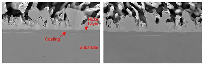
Functions of Each Layer
1. Nickel (Ni) Layer: Barrier Layer
Core functions: Block copper diffusion to the surface, restrain excessive formation of Au-Cu intermetallic compounds, provide mechanical strength and boost corrosion resistance.
Without a nickel barrier layer, copper oxidizes easily, resulting in reduced bond pull strength and degraded long-term reliability.
2. Palladium (Pd) Layer: Protective Intermediate Layer
Palladium acts as a critical interlayer between nickel and gold to prevent nickel oxidation.
Exposed nickel readily generates nickel oxides (NiO, Ni₂O₃), which hinder the formation of sound gold ball bonds and lower ball shear strength.
Meanwhile, palladium isolates oxygen and greatly mitigates the risk of black pad defects.
Electroless nickel immersion gold (ENIG) commonly suffers Ni-P corrosion, which causes bond lifting and brittle solder joints.
A palladium layer effectively shields nickel, drastically cutting such risks and improving long-term reliability.
Common qualification tests covering reliability: 85°C/85%RH temperature-humidity bias test, HAST, salt spray test.
3. Gold (Au) Layer: Bonding Layer
Gold wires directly contact the gold layer.
Gold is oxidation-free, facilitates uniform gold ball formation, delivers low contact resistance and offers a wide bonding process window.
However, excessive gold thickness raises costs. Thick gold plating also encourages thick intermetallic layer growth during wire bonding.
Therefore, only an ultra-thin gold coating is deposited for Ni/Pd/Au finishes.
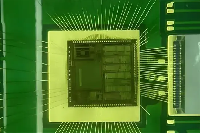
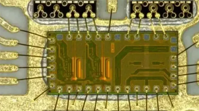
Why Optical Modules Specifically Require Ni/Pd/Au Finish
Optical modules operate in data centers, telecommunications networks and outdoor equipment with long service life requirements (typically 10 to 25 years).
They must endure harsh operating environments featuring high temperature & humidity, sulfur-containing gases, salt mist and thermal cycling.
Standard hard gold plating or ENIG finishes often fail to meet stringent reliability standards, making Ni/Pd/Au the mainstream surface treatment solution.
Corrosion Resistance Considerations for Wire Bonding
The industry enforces the following standardized corrosion tests:
High Temperature & High Humidity Test Standard condition: 85°C / 85% RH for 1000 hours.
Evaluations include bond pull force, ball shear strength and contact resistance after testing.
Salt Spray Corrosion Test Standard condition: 5% NaCl solution at 35°C. Inspect for gold layer perforation and nickel substrate exposure.
Sulfidation Corrosion Test Exposure to H₂S and SO₂ gas.
Silver wires are highly susceptible to sulfidation, while gold wires demonstrate superior stability.
Electrochemical Migration Under high humidity, gold and copper ions migrate across the surface, easily triggering leakage current and electrical short circuits. Ni/Pd/Au plating effectively suppresses such risks.
Standard Thickness Specifications of Ni/Pd/Au for Optical Modules
General Ni/Pd/Au thickness stack-up: Ni (3–7 μm) + Pd (0.05–0.15 μm) + Au (0.03–0.1 μm).
Typical stack-up for high-speed optical modules (100G/400G/800G): ~5 μm Ni + 0.1 μm Pd + 0.05 μm Au.
Common Diameter Sizes of Gold Bonding Wires for Optical Modules
Gold wire gauge is determined by operating current, signal frequency, pad pitch and chip dimensions.
0.8 mil (20 μm): Widely used for Driver IC, TIA IC and EML Driver bonding.
1.0 mil (25 μm): The most universal size for general optical transceiver products.
1.2 mil (30 μm): Applied to assemblies carrying high operating currents.
For telecom-grade optical modules compliant with Telcordia GR-468, the industry standard stack-up in mass production is: 3–5 μm Ni + 0.08–0.15 μm Pd + 0.03–0.08 μm Au paired with 0.8–1.0 mil gold wire.
This configuration balances high wire bonding yield, robust corrosion resistance and long-term reliability requirements exceeding 20 years of service life.