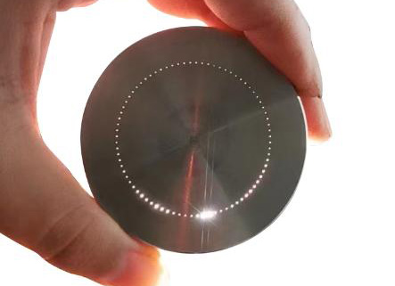
In the field of micro- and nano-manufacturing, the precision of apertures directly determines product performance.
From the micron-sized flow channels of aerospace fuel nozzles to the nanopore arrays on the surface of medical scaffolds, laser microvia machining technology is driving precision manufacturing to the submicron level.
This paper analyzes the principle, technical difficulties, mass production applications and cutting-edge direction.
Processing principle:
heat conduction and nonlinear absorption mechanism
Traditional laser hole processing relies on the thermal effect of nanosecond pulsed laser, through the material melting or vaporization to achieve hole formation.
This type of process is suitable for hole diameters ranging from millimeters to hundreds of microns. However, carbonization and microcracks caused by the heat-affected zone (HAZ) limit its use in sensitive applications, such as semiconductor wafers and biological materials.
Ultrafast lasers (femtosecond/picosecond class) change the processing mode through a nonlinear absorption mechanism:
Multiphoton ionization dominates material removal when the pulse width is shorter than the material electron-lattice thermal relaxation time (<10 ps).
For example, femtosecond laser processing of fused silica, the focal region generates plasma, realizing sub-micron precision, near-zero thermal damage cold processing, and the hole wall roughness can be controlled at Ra<0.1 μm.
Technical difficulties:
Currently, the main technical bottlenecks are concentrated in two aspects:
1.Depth-to-diameter ratio limitations
When the processing depth of Gaussian beam exceeds 500 μm, the Rayleigh length limitation leads to insufficient energy at the bottom of the hole.
The use of Bessel beams, which have non-diffracting properties, can increase the effective machining depth by 3–5 times. For example, in MEMS pressure sensor deep-hole processing, a depth-to-diameter ratio of 50:1 has already been achieved.
2.Complex structure molding
Microfluidic chips need to be tapered holes, spiral holes and other shaped structures.
Through the spatial light modulator (SLM) dynamic modulation of the wavefront phase, programmable control of the laser focus three-dimensional trajectory.
A German research institute in the PDMS material processed cone angle precision ± 0.5 ° micro-flow channel, fluid efficiency increased by 40%.
Mass production applications:
Mass production process needs to consider the accuracy and economy:
1.Automobile fuel injector processing
Using green nanosecond laser (pulse width 20 ns), single hole processing time <50 ms, average daily capacity of 100,000 holes, the cost of 0.02 yuan / hole;
2.Heart stent microporous processing
Femtosecond laser (pulse width 300 fs) with gas-assisted system, in 316L stainless steel surface processing diameter 30 ± 2 μm microporous, heat-affected zone <2 μm, but the cost of equipment exceeds 5 million yuan, the cost of a single hole 1.2 yuan.
3.Composite processing technology has become a new trend
For example, Japan’s Fanuc uses a laser-electrolytic composite process: first, nanosecond laser pre-processing is performed, followed by electrochemical polishing. This reduces the hole wall roughness from Ra 3.2 μm to 0.4 μm, with a sixfold increase in efficiency.
Frontier direction:
Ultra-fast laser in transparent materials within the three-dimensional modification capabilities are expanding application scenarios:
1, the U.S. Lawrence Laboratory in the sapphire internal processing of 5 μm diameter, depth of 1.2 mm three-dimensional micro-channels for high-power laser heat dissipation;
2, The Chinese Academy of Sciences, Xi’an Institute of Optical Machinery, developed laser-induced reverse deposition (LIRD) technology. This technology generates a silicon nitride insulating layer on the inner walls of micro-holes. It is applied to terahertz waveguide devices.
When the aperture reaches the submicron scale, the process shifts from physical material removal to precise manipulation of quantum effects. These include electronic states and photonic-phonon coupling.
New tools like attosecond lasers and topological beams are driving advances in micro- and nanohole processing. This technology is breaking the classical optical limit. It lays the foundation for future industries such as quantum chips and bionic organs.
In this game of precision and cost, Chinese manufacturers face a key challenge. They must achieve breakthroughs in core components like ultrafast lasers and high-precision motion platforms. Whether they succeed will determine the future landscape of global micro-nano manufacturing.
Conclusion
Laser microvia machining is at the forefront of precision manufacturing, continuously pushing the boundaries of micro- and nano-scale fabrication.
The shift from nanosecond pulsed lasers to ultrafast femtosecond lasers has enabled near-zero thermal damage processing. This achieves submicron precision, which is crucial for advanced applications in aerospace, medical devices, and semiconductor manufacturing.
Despite significant advancements, key technical challenges remain, particularly in achieving high aspect ratios and complex 3D structures.
Innovations such as Bessel beams, spatial light modulators, and hybrid processing techniques are addressing these limitations, enabling mass production with improved efficiency and cost-effectiveness.
Looking ahead, the integration of ultrafast laser processing with emerging quantum and photonic technologies is set to redefine the possibilities of micro- and nanofabrication.
The ability to manipulate electronic states and photonic interactions at the submicron level will open doors to next-generation applications, from quantum chips to bionic materials.
For Chinese manufacturers, the ability to develop core technologies—such as high-performance ultrafast lasers and precision motion platforms—will be a decisive factor in shaping the global landscape of micro-nano manufacturing.
As competition grows, breakthroughs in these areas will boost industrial capabilities. They will also help establish leadership in the future of precision engineering.